S100 Computers

Home S-100 Boards History New Boards Software Boards For Sale
Forum Other Web Sites Quiz Index    

BRINGING UP CPM3 FOR THE FIRST TIME ON A IDE HARD DISK BASED SYSTEM.
Before you read this page please read about bringing up CPM3 on a Floppy Disk based system first. Please see here.  After reading that page some parts of this page will appear the same. However there are subtle and important differences, so read carefully.  Throughout I will refer to a Hard Disk.  Please keep in mind that everything said below also applies to CF card "Disks" utilizing an IDE to CF card adaptor as described here.

To repeat what was said on the Floppy disk page. Most early S-100 Computer systems used CPM2.2 (or earlier) as the basic computer disk operating system.  The system was fairly simple to implement and was the germination base for much of the microcomputer worlds software.  The system however had many limitations. In particular it was designed for a standard 8" IBM single density single sided floppy disk with 128 byte sectors.  As newer disk sizes and formats started to appear -- particularly hard disks, the system started to show its limitations.  Digital Research's answer was CPM3.  This version of CPM allowed essentially any sector size and disk format to be used easily and efficiently.  What CPM3 did was hide within the operation system itself the 128 byte sector size requirement and allow the BIOS to work easily with any sector size "transparently". The system had an  elaborate disk hashing/data buffering system as well. 

Of particular usefulness was the fact that it existed in two forms. A "standard" NON BANKED version that operated like CPM2.2 in a Z80 system with 64K (or less) of RAM. However there was a much more efficient "BANKED" version of CPM3 which by using onboard 'bank switching" hardware, could utilize up to (in theory) many megabytes of RAM. Typically 128K or 256K RAM systems were used.   This allowed for a very fast and sophisticated system. 

It should be noted that this BANKED system absolutely requires that the Z80 can switch in and out a portion of its 64K address space with other RAM boards.  There were a number of ways this was done in hardware.  The Cromemco and Godbout systems utilized an IO port to switch RAM boards.  Intersystem's and our own S100Computes/N8VRAM Z80 board, use on-board Z80 CPU board hardware to extend the addressing range of the Z80.  We will discuss this later.

We will first start with a very simple CPM3 BIOS (for a <64K RAM), single hard disk based system.  We will step by step build the system up to a much more complex setup. Eventually arriving at a BANKED system with multiple hard disks, floppies, and memory disk connections.  


Writing a simple CPM3 BIOS for the S-100Computers/NVRAM IDE Board
Before we start if would be very helpful if you first look over the very detailed description Digital Research provide in their CPM3 BIOS configuration manual. One word of warning!  This manual (CPM3 System Guide),  is extremely detailed and contains far more detail than is typically needed. It explains in great detail how the disk parameter tables are setup etc.  When you read this for the first time you may run away. Hang in there, Digital Research provided a number of assembler macro routines that do all the dirty configuration work for you. They also provided an interactive "GENCPM" program that via a series of questions and answers makes and configures a complete system for you.  Thanks to PC Pete's for the CPM3 System guide. We now also have from him beautiful copies of the Digital Research CPM3 User Guide, Programmers Guide and Command Guide.

While it is useful (and comforting), you really don't have to know about many of the underlying process in writing a CPM3 BIOS. Your job as we will see, is simply to write 5 core modules for the hard disk hardware to:-

Initialize the IDE hard disk (or CF card) drive
Log in a drive
Read a sector
Write a sector.
Write a "DPH" table that describes the hard disk format


These modules have to be bullet proof, but that's it. The Digital Research GENCPM will do the rest.

Here is a diagram of the steps involved in booting up CPM3 from a hard disk:-

CPM3 HD boot process
 
We will write software for all these steps.  Normally I have seen the process written from the bottom up. I think it is in fact easier to understand if we go from the top down.

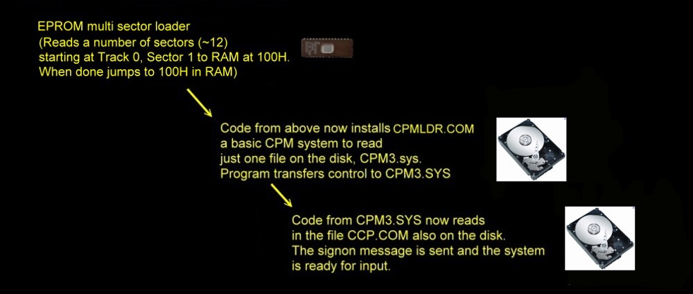
THE EPROM MULTI SECTOR HARD DISK BOOT LOADER.
The first difference between a Floppy and Hard Disk system is that the CPMLDR (see below) boot process is a little simpler. Rather than read in one sector from the disk (to get disk parameters etc.) and then from that sector load in the remaining sectors,  in the case of Hard disks it is common to read in all of the CPMLDR sectors at once via the EPROM Boot Loader. This is because in the case of a hard disk the format is fixed and we always know how many actual sectors are required. In the case of floppy disks the number varies depending on the sector size.  Once the CPMLDR is present in RAM at 100H upwards control is transferred to it.

The code at 100H is RAM is really a stripped down very compact CPM operating system (called CPMLDR.COM)  that's only function in life is to read is a single CPM file on the disk named CPM3.SYS.  It has to be a "proper" CPM operating system however because the CPM3.SYS file is a "normal" CPM file and can exist anywhere on the disk.   In a Non-Banked system this CPM3.SYS 
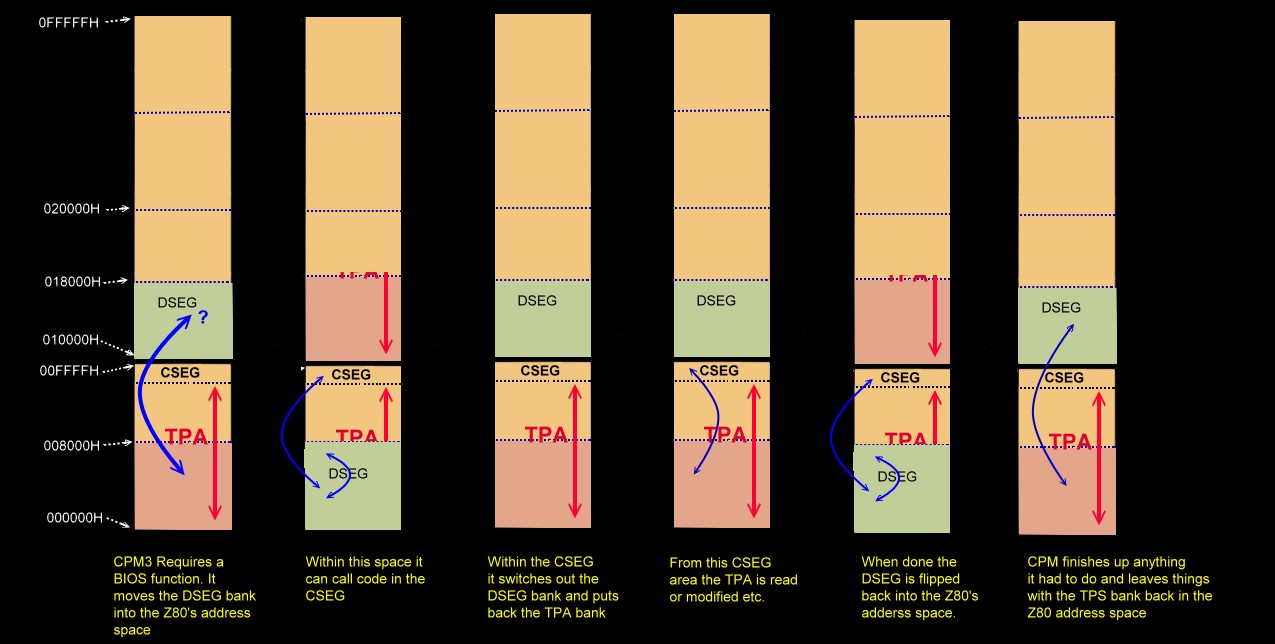
code is placed in the top of RAM. In a Banked system much of it is placed in another RAM bank - thus freeing up much of the TPA. More on that later.

We are almost home. The last step in the process is the CPM3.SYS code itself reads in a further CPM3 file called CCP.COM. This Console Command Processor  file has the code that links the operating system with the outside world (console, printer etc).  When this is done the CPM3.SYS code transfers control to the CCP.COM code and the A:> appears.

This my seem a convoluted way of doing things -- and to some extent it is, however what is really nice is that once you have the original CPMLDR working you can easily and quickly make changes to the operating system by placing a new CPM3.SYS file on the disk.  If you change the name (CPM always looks for exactly "CPM3.SYS") you can have different hardware arrangements stored on the same hard disk.

Now let us look at an example of the EPROM boot loader code.  My complete "MASTER.Z80" EEPROM code can be see here. See the bottom of this page for all downloads. The relevant Hard Disk boot loader code begins at HBOOTCPM:   This is the monitor I use with the S100Computers/N8VRAM Z80 CPU board.  It utilizes the simple command driven interface to read disk sectors into RAM utilizing the IDE board.  Other hard disk controller boards would behave essentially the same way.
 
;-------------- BOOT UP CPM FROM HARD DISK ON S100COMPUTERS IDR BOARD ----------------
 
;BOOT UP THE 8255/IDE Board HARD DISK/Flash Memory Card
 
HBOOTCPM:
        POP     HL                     ;CLEAN UP STACK
        LD      HL,SPEAKCPM_MSG        ;Announce on speaker
        CALL    SPEAK$
        
        CALL    INITILIZE_IDE_BOARD    ;Initialize the 8255 and drive (again just in case)
 
        LD      D,11100000B            ;Data for IDE SDH reg (512bytes, LBA mode,single drive)
        LD      E,REGshd               ;00001110,(0EH) CS0,A2,A1,  
        CALL    IDEwr8D                ;Write byte to select the MASTER device
 
        LD      B,0FFH                 ;Delay time
WaitInit:      
        LD      E,REGstatus            ;Get status after initilization
        CALL    IDErd8D                ;Check Status (info in [D])
        BIT     7,D
        JR      Z,SECREAD              ;Zero, so all is OK to write to drive
                                       ;Delay to allow drive to get up to speed
        PUSH    BC
        LD      BC,0FFFFH      
DXLAY2: LD      D,2                    ;May need to adjust delay time to allow cold drive to
DXLAY1: DEC     D                      ;to speed
        JR      NZ,DXLAY1
        DEC     BC
        LD      A,C
        OR      B
        JR      NZ,DXLAY2
        POP     BC
        DJNZ    WaitInit
IDError:
        LD      HL,DRIVE_NR_ERR        ;Drive not ready
        JP      ABORT_ERR_MSG
 
SECREAD:                               ;Note CPMLDR will ALWAYS be on TRK 0,SEC 1,Head 0
        LD      A,11111111B            ;FLAG PROGRESS VISUALLY FOR DIAGNOSTIC
        OUT     (DIAG_LEDS),A
 
        CALL    IDEwaitnotbusy         ;Make sure drive is ready
        JR      C,IDError              ;NC if ready
 
        LD      D,1                    ;Load track 0,sec 1, head 0
        LD      E,REGsector            ;Send info to drive
        CALL    IDEwr8D
 
        LD      D,0                    ;Send Low TRK#
        LD      E,REGcyLSB
        CALL    IDEwr8D
 
        LD      D,0                    ;Send High TRK#
        LD      E,REGcyMSB
        CALL    IDEwr8D
 
        LD      D,SEC_COUNT            ;Count of CPM sectors we wish to read
        LD      E,REGcnt
        CALL    IDEwr8D
 
        LD      D,CMDread              ;Send read CMD
        LD      E,REGCMD
        CALL    IDEwr8D                ;Send sec read CMD to drive.
        CALL    IDEwdrq                ;Wait until it's got the data
 
        LD      HL,CPM_ADDRESS         ;DMA address where the CPMLDR resides in RAM
        LD      B,0                    ;256X2 bytes
        LD      C,SEC_COUNT            ;Count of sectors X 512
MoreRD16:
        LD      A,REGdata              ;REG register address
        OUT     (IDECport),A   
 
        OR      IDErdline              ;08H+40H, Pulse RD line
        OUT     (IDECport),A   
 
        IN      A,(IDEAport)           ;read the LOWER byte
        LD      (HL),A
        INC     HL
        IN      A,(IDEBport)           ;read the UPPER byte
        LD      (HL),A
        INC     HL
        
        LD      A,REGdata              ;Deassert RD line
        OUT     (IDECport),A
        DJNZ    MoreRD16
        DEC     C
        JR      NZ,MoreRD16
 
        LD      E,REGstatus            ;Check the R/W status when done
        CALL    IDErd8D
        BIT     0,D
        JR      NZ,IDEerr1             ;Z if no errors
        LD      HL,STARTCPM
        LD      A,(HL)
        CP      31H                    ;EXPECT TO HAVE 31H @80H IE. LD SP,80H
        JP      Z,STARTCPM             ;AS THE FIRST INSTRUCTION. IF OK JP to 100H in RAM
        JP      ERR_LD1                ;Boot Sector Data incorrect
 
IDEerr1:
        LD      HL,IDE_RW_ERROR        ;Drive R/W Error
        JP      ABORT_ERR_MSG
 
        
;      ----- SUPPORT ROUTINES --------------
 
INITILIZE_IDE_BOARD:                  ;Drive Select in [A]. Note leaves selected drive as [A]
        LD      A,RDcfg8255           ;Config 8255 chip (10010010B), read mode on return
        OUT     (IDECtrl),A           ;Config 8255 chip, READ mode
                              
                                      ;Hard reset the disk drive 
                                      ;For some reason some CF cards need to the RESET line 
                                      ;pulsed very carefully. You may need to play around   
        LD      A,IDEreset            ;with the pulse length. Symptoms are: incorrect data coming
        OUT     (IDECport),A          ;back from a sector read (often due to the wrong sector being read)
                                      ;I have a (negative)pulse of 2.7uSec. (10Mz Z80, two IO wait states).
        LD      B,20H                 ;Which seem to work for the 5 different CF cards I have
ResetDelay:
        DEC     B
        JP      NZ,ResetDelay          ;Delay (reset pulse width)
 
        CALL    DELAY_32               ;Need to stretch pulse!
        XOR     A
        OUT     (IDECport),A           ;No IDE control lines asserted (just bit 7 of port C)
 
IDEwaitnotbusy:                        ;Drive READY if 01000000
        LD      B,0FFH
        LD      C,80H                  ;Delay, must be above 80H for 4MHz Z80. Leave longer for slower drives
MoreWait:
        LD      E,REGstatus            ;Wait for RDY bit to be set
        CALL    IDErd8D
        LD      A,D
        AND     11000000B
        XOR     01000000B
        JR      Z,DoneNotbusy  
        DJNZ    MoreWait
        DEC     C
        JR      NZ,MoreWait
        SCF                           ;Set carry to indicate an error
        RET
DoneNotBusy:
        OR      A                      ;Clear carry it indicate no error
        RET
                                       ;Wait for the drive to be ready to transfer data.
                                       ;Returns the drive's status in Acc
IDEwdrq:
        LD      B,0FFH
        LD      C,0FFH                 ;Delay, must be above 80H for 4MHz Z80. Leave longer for slower drives
MoreDRQ:
        LD      E,REGstatus            ;wait for DRQ bit to be set
        CALL    IDErd8D
        LD      A,D
        AND     10001000B
        CP      00001000B
        JR      Z,DoneDRQ
        DJNZ    MoreDRQ
        DEC     C
        JR      NZ,MoreDRQ
        SCF                           ;Set carry to indicate error
        RET
DoneDRQ:
        OR      A                      ;Clear carry
        RET
;
;------------------------------------------------------------------
; Low Level 8 bit R/W to the drive controller.  These are the routines that talk
; directly to the drive controller registers, via the 8255 chip.  
; Note the 16 bit I/O to the drive (which is only for SEC Read here) is done directly 
; in the routine MoreRD16 for speed reasons.
 
IDErd8D:                              ;READ 8 bits from IDE register in [E], return info in [D]
        LD      A,E
        OUT     (IDECport),A           ;drive address onto control lines
 
        OR      IDErdline              ;RD pulse pin (40H)
        OUT     (IDECport),A           ;assert read pin
 
        IN      A,(IDEAport)
        LD      D,A                    ;return with data in [D]
 
        LD      A,E                    ;<---Ken Robbins suggestion
        OUT     (IDECport),A           ;Deassert RD pin
 
        XOR     A
        OUT     (IDECport),A           ;Zero all port C lines
        RET
 
 
IDEwr8D:                              ;WRITE Data in [D] to IDE register in [E]
        LD      A,WRcfg8255            ;Set 8255 to write mode
        OUT     (IDECtrl),A
 
        LD      A,D                    ;Get data put it in 8255 A port
        OUT     (IDEAport),A
 
        LD      A,E                    ;select IDE register
        OUT     (IDECport),A
 
        OR      IDEwrline              ;lower WR line
        OUT     (IDECport),A
 
        LD      A,E                    ;<-- Kens Robbins suggestion, raise WR line
        OUT     (IDECport),A
 
        XOR     A                      ;Deselect all lines including WR line
        OUT     (IDECport),A
 
        LD      A,RDcfg8255            ;Config 8255 chip, read mode on return
        OUT     (IDECtrl),A
        RET
 

As I explained above, we have just read in 12 sectors to RAM starting at 100H.  Note how the HBOOTCPM in this case jumps to 100H in RAM once all 12 sectors have been read. It is here the CPMLDR for our hard disk CPM3 system now resides.

THE CPMLDR  LOADER.
Next we will write the CPM Loader program CPMLDR.COM. This is actually the hardest part of the software to write. We are is essence writing a primitive CPM3 BIOS for the hard disk. The good news is we don't worry about memory banking, and only have to take care of two major BIOS functions, reading sectors from (only) the Hard Disk and writing to the console. You don't even need console input -- though it is useful for debugging.
 
The complete Loader BIOS for the IDE board (HLDRBIOS.Z80) can be seen here.  Before we get into it, we need to discuss how CPM3 understands disk formats.

In CPM3 each disk has its own Disk Parameter Block  table.  Unfortunately these tables (DPB's) are fairly complex and rather than repeat everything here, you should read the Digital Research CPM3 System Guide mentioned above.  They contain byte and word values to define areas in RAM for sector skew translation, directory buffers and hash tables etc.   We will not worry about any of this now because Digital Research provides a series of Assembler macros that builds these tables automatically for you. 

For our hard disk the DPB macro is:-

HD$DPB:     DPB 512,61,256,2048,1024,1,8000H

 512   = Bytes per sector
   61   = Sectors per track
 256   = Tracks per disk
2048  = The allocation unit size (2K blocks for our hard disk)
1024
  = Maximum number of directory entries on a disk
     1   = Number or tracks reserved for the CPM operating system.
8000H= Special flag to indicate disk is permanent/hard disk

Tracks start at 0,1,2,3,.. so track 0 is reserved for the operating system. The disk directory starts on Track 1 in our case.
You will see this macro at the bottom of the above code listing.

Next we need another table which Digital Research calls a Disk Parameter Header  table or DPH.  This table is somewhat simpler than in the case of the 8" floppy disk DPH table. This time we do not need to use a sector skew so the first entry. So it is set to 0.

In fact the only thing this table contains is a pointer to the above DPB table.   Again an assembler macro is supplied. 
For our hard disk the DPH macro is:-

DPH0:      DPH      0,HD$DPB,0,

0                    For floppies this entry points to the "skew" macro that describes how the sectors are numbered on a track (it is not used here).
HD$DPB         Is a word pointer to the above DPB for the hard disk.
                  This is the maximum size in bytes of the disk checksum vector, lets skip for now
0                    This is the maximum size in bytes of the disk allocation vector, lets skip for now also and just use these values


OK we are almost there. There is still yet one more table.  This is the Disk Drive Table or DTBL

This one is simple.  CPM3 allows for up to 16 different drives.  The DPH table is just a list of pointers to each DPH for each drive. Any entries with no drive are set to 0.    We have only one drive here. So the DTBL will be:-

@DTBL:       DW    DPH0,0,0,0,0,0,0,0,0,0,0,0,0,0,0,0

When you look at the bottom of the code for the CPMLDR "BIOS" (HLDRBIOS.Z80) you will see all of the above combined. For more efficient use of code space I have actually hand coded the DPH table.

Now in order to have a functional basic operating system we need to splice in the Digital Research CPMLDR.REL file.  This a disk operating system file supplied by Digital Research that works with our basic custom BIOS.   Remember all we are trying to do here is read in the main CPM3.SYS file on the disk.  The CPMLDR.REL file is set to run at 100H in RAM.   It is constructed such that it expects immediately above it the Loader BIOS jump vectors exactly as they are at the start of HLDRBIOS.ASM.

We use the CPM program LINK to splice the two sections together and write them out as one file CPMLDR.COM.

If you load this program with SID or ZSID and jump to 100H in RAM the above code should work and come back telling you it cannot locate the CPM3.SYS file on the disk. (Because we have not done it yet).

However before we get to that we have to do one other thing. We need to get some way to write the CPMLDR.COM file to tracks 0  of the hard disk.

I have written the program HSYSGEN.Z80 to do this.  It can be seen here.  Its essentially a reverse of the EPROM monitor code to write (rather than read) multiple sectors to the disk.

Finally we need to splice the HSYSGEN and CPMLDR code together to yield one "standard"  CPM program which I call HSYSGEN.COM This program on any of our IDE disks or CF cards will place the above CPMLDR.com code on the system tracks.

The code is a little bit more complicate than I described above because it has the option of placing a Banked or Non-Banked CPMLDR.COM file on the disk. For now everything will be for a non-banked system.

All of the above assembly and splicing can be done automatically by running the HSYSGEN.SUB file. This can be see here.


THE CPM3.SYS FILE.
This file is the heart of the operating system.  First we need to decide how we will layout our hardware. For our first system we will just have a Console and one hard disk A:

First we will work on the Hard disk portion of the BIOS. This is contained in the file HIDE3.ASM.  The source code can be seen here. The BIOS contains essentially the same tables that I described above and uses the same assembler macros.  However there is one more new table structure it is called the Extended Disk Parameter Table (XDPH).   The XDPH is in fact nothing more than the above DPH table except that additional bytes and word parameters are placed immediately before and ( if required), after, the "regular" DPH table described above.  However the exact placement of these extra parameters is very critical.  Here is the XDPH table I use for drive A:
; EXTENDED DISK PARAMETER HEADER FOR DRIVE 0: (A:)
	DW	HDWRT		;HD SEC WRITE ROUTINE
	DW	HDRD		;HD SEC READ ROUTINE
	DW	HDLOGIN		;HD LOGIN PROCEDURE
	DW	HDINIT		;HD DRIVE INITIALIZATION ROUTINE
	DB	0		;RELATIVE DRIVE 0 ON THIS CONTROLLER
	DB	0		;MEDIA TYPE KNOWN 
				;HI BIT SET : DRIVE NEEDS RECALIBRATING
DPH0:	DPH 0,IDEHD$DPB,0,
IDEHD$DPB  DPB 512,61,256,2048,1024,1,8000H

You can see the normal DPH begins at DOH0:  Listed above it are two byte fields (unused here) that the software can use as flags for floppy disk density/format etc.  CPM does not use them. Then immediately above them are four word pointers to disk the initialization, login, sector read and write routines.  These are the routines you must custom  write for each disk.  CPM also adds table values to the bottom of the DPH. In fact from the location DPH0: the next 24 bytes must never be changed by your custom BIOS. You can add any other flags or pointers you like below that. I use two in all my floppy disk BIOS'es but we don't need any here.

Take a look over the HIDE3.ASM code to get comfortable with the above.   You should by now be familiar with the disk DPH and DPB macros.
 
Next we need to look at the HDRVTBL2.ASM file.  This one is simple.  It just contains the DTBL we described above.  We have only one  disk whose DPH's are labeled DPH0 so we see:-

  @DTBL:        DTBL <DPH0,0,0,0,0,0,0,0,0,0,0,0,0,0,0,0>

BTW, throughout these programs, Digital Research names all data pointers/variables  beginning with a "@'. All public routines  are labeled with an  '?'.  So ?PMSG is a globally available routine to print a message on the console.

Next we have CHARIO3.ASM. As you might expect from the name this file concerns itself with getting data to and from the Console (and printer).  There are elaborate mechanisms is CPM3 to set serial Baud rates etc. For this simple case just go to the bottom of the file and splice in code for your particular hardware.  The code there is actually more complicates than need be because I have options to redirect output to two printers and the like. Be sure you use the correct  I/O port equates for your hardware however.

Then we have HBOOT3.ASM.  The only function of this file in our simple system is to place an initial signon message on the  screen when CPM3 signs on for the first time.   If you have various system/hardware configurations, the message at the bottom of the file is a useful place to put reminders.

So except for HIDE3.ASM  and CHARIO3.ASM , the changes you will have to make for any hardware system are fairly simple.
The other files BIOSKRNL.ASM,  SCB3.ASM,  MOVE3.ASM are not modified in this simple system.  

We assemble and link all of the above .ASM  files together to make our CPM3 custom BIOS file called BIOS3.SPR

Next we need one other supplied Digital Research file: BDOS.SPR. This file contains the code for the core disk operating (BDOS) system that Digital Research supplied.

We then utilize the special CPM3 program Digital Research supplied called GENCPM.COM. This program will take the above BDIOS3.SPR and BIOS3.SPR files and combine them to make our final CPM3.SYS file.  GENCPM is an interactive program. It will ask you a number of questions about how exactly you would like your custom CPM3 operating system to function.  Things like do you want long error messages, which disk you want as the boot/primary disk, how much space to set aside for directory buffers etc.

Fortunately Digital Research provided good examples.  The input for the GENCPM program can be read from a GENCPM.DAT file. This saves you typing in the same values each time.  I provide a sample GENCPM.DAT here.

The above process actually appear here more complex than it actually is.  I have written the following CPM submit file that will do all of the above with a one line entry the Windows Altair CPM emulator box on the I: Drive.
Just type:-

submit HMAKECPM

The final CPM3.SYS file should appear in your windows directory from where you launched Altair.com

Here is a listing of that HMAKECPM.SUB file:-

;r RMAC.COM
;r LINK.COM
;r GENCPM.COM
;
;
r GENCPM.DAT
;
r Z80.LIB
r CPM3.LIB
r MODEBAUD.LIB
;
r BIOSKRNL.ASM
r BDOS3.SPR
;
r SCB3.ASM
r CHARIO3.ASM
r MOVE3.ASM
;
r Hboot3.asm
r Hdrvtbl3.asm
r Hide3.asm
;
RMAC BIOSKRNL.ASM
;
RMAC SCB3.ASM
RMAC CHARIO3.ASM
RMAC MOVE3.ASM
;
RMAC HBOOT3.ASM
RMAC HDRVTBL3.ASM
RMAC HIDE3.ASM
;
;A: is the IDE Drive (Only disk!)
;
LINK BIOS3[B]=BIOSKRNL,SCB3,HBOOT3,CHARIO3,MOVE3,HDRVTBL3,HIDE3
;
;Note GENCPM.DAT holds previous values
;This will be a Non-Banked version. IDE Drive on A:
;
gencpm auto
;
w cpm3.sys B
;
; Note this version is NON-BANKED and for a single IDE Drive only


You next need to transfer the above CPM3.SYS file to your IDE disk /CF card. If you first did a Floppy disk CPM3 system this is easy.  For people that don't have any way of transferring files to their first CF card, I can do it for them if they send on a blank card and software.

Finally you need to also transfer to this same disk  the Digital Research supplied CCP.COM program.

With your CPMLDR code already on the disks system tracks as describe above and the two files CPM3.SYS and CCP.COM listed in the disks directory you are ready to boot CPM3!

If it does not work, first from an old floppy system try loading the CPMLDR file into RAM with SID. Switch disks and go to 100H.   The system should boot. If it does there is a problem with your boot loader. 

Alternatively you can boot from an 8"  Floppy disk with a non banked floppy based version of CPM3 as described here, but instead of using the floppy CPM3.sys file place the Hard Disk CPM3.sys file described above on the floppy disk. It should come up with the hard disk on drive A:   If you still have problems then back off and modify you floppy based system such that your Hard Disk is drive C: This way form a working floppy system you can debug the IDE Hard Disk on drive C: using the diagnostic program MYIDE.ASM.  Also the old public domain CPM disk diagnostic program "DU.COM" is quite useful for seeing sector contents as CPM understands them.  Remember however you must be using a non-banked floppy based CPM3 system.

If you still have problems then use the approach of sprinkling your BIOS code with Console  character outputs (direct to hardware, not via CPM) at various points to see where the problem lies.  One nice thing about the new IDE board (Version 3) is you can always see what drive, track and sector is being addressed.   Directory reads for example are on Track 1.  The boot loader should start on Track 0 and step along all the way up to Track 1, sector 0CH.


A SIMPLE BANKED CPM3 VERSION FOR A SINGLE IDE HARD DISK/CF CARD.
Next we will move up to a banked version of CPM3 in the same system.   As I said above, CPM3 comes in two flavors. A "Non-Banked" system where up to 64K of RAM  can be utilized to run the operation system and application(s).  The second much more powerful approach is a "Banked" system. This utilizes two or more S-100 memory cards to switch in or out various blocks of memory and yet still remain within the 64K memory addressing capability of the Z80. Typically the bank is a 16 or 32K block of RAM that transitions in or out of the CPU's 16 bit address space.   These banks can be port selected utilizing the S-100 phantom line and/or by activating and inactivation a port on certain S100 RAM boards which by using onboard 'bank switching" hardware, could utilize up to (in theory) many megabytes of RAM. Typically 128K or 256K RAM systems were used.   This allowed for a very fast and sophisticated system. 

It should be noted that this BANKED system absolutely requires that the Z80 has hardware that can switch in and out a portion of its 64K address space with other RAM boards.  There were a number of ways this was done in hardware.  The Cromemco and Godbout systems utilized an IO port to switch RAM boards.  Intersystem's and our own S100Computes/N8VEM Z80 board, use on-board Z80 CPU board hardware to extend the addressing range of the Z80. 
The two types of approaches can be diagramed as follows:-

Extended Addressing modes

They both behave the same in terms of software. Digital Research referred to these "extra" memory blocks of RAM as "Banks".  In a typical CPM3 Banked system there are usually two, sometimes 3 banks.  Where these banks "split" in the Z80's 64K address space varies with the hardware.  With our S100Computers Z80 board this is completely determined by software. Not so typically, in I/O port driven systems. A common split is at the 8000H or C000H boundary. 
Here is a typical Bank CPM3 setup:-
 
CPM3 Memory layout
 
In a banked CPM3 system, the Monitor/EPROM Boot loads the CPM3
CPMLDR.COM  from the disk system tracks into RAM at 100H exactly as described above for the non-banked system.   However once control is passed to the CPMLDR at 100H in RAM,  things go differently.  The first thing the loader does in a banked system is open up an alternative bank of RAM above/outside the Z80's 64K address space.  As I said above this is quite hardware dependent and varies from system to system.

In our S100Computers Z80 board's case we will move the RAM contents from 0H to 7FFFH up to 10000H to 17FFFH.  In Digital Research terminology, we call the RAM from 10000H-17FFFH Bank 0.  We call the "old" RAM at 0-7FFFH Bank 1.  Using the boards hardware we then flip banks  so the RAM contents change as is shown here:-
 
Bank Switching


It's very important to understand that the Z80 itself does not know anything has happened.  It all the time sees one large block of 64K RAM. In fact while it thinks it is operating on RAM 0  to ~4K it is in fact using RAM from 1000H upwards ~4K.

The CPMLDR then loads in the main CPM3.SYS file from the disk as we described above for the non-banked system but this time instead of dumping everything in high memory,  it distributes the contents both in high memory (a small portion) and the rest in our Bank 1 memory (the major portion of code).   How CPM does this we will discuss in a moment.  What part goes where is the tricky part of writing a good CPM3 BIOS.  In all the BIOS code we will look at you will see chunks assigned to "Common Memory Segments"
(CSEG's) or "Data Memory Segments" 
(DSEG's).  CSEG portions of the BIOS code always reside above and outside the Banked switching region of RAM in high memory.  They never change, any addresses are absolute and can always count on being there.   In other words the code behaves like Non-Banked BIOS code.    DSEG BIOS code on the other hand resides in Bank 0 RAM (or other Banks). Nothing special about the code itself within this segment either. 

What is special is when you jump back and forth between code in DSEG RAM and CSEG RAM.  Before you make a jump say from code in DSEG to a CSEG, you need to save the current bank number, switch banks so Bank1 is contiguous with the CSEG code above the bank switching area in high memory and then jump from that DSEG (now in the contiguous 64K RAM space) to CSEG code in high RAM.  This is necessary because remember the Z80 never knows banks are switched. If the code in CSEG just jumped to a region below the bank boundary it would not find the CSEG code there.  (It is in fact, way up above 10000H in RAM).

Here is a diagram of the process:-

The CPM banking Process
 

Let us look at a small code snipped from the BIOS Hard Disk sector read routine.  Most of the BIOS code will be in banked RAM and so DSEG.  However when we get to the part where we are actually reading in data bytes from the FDC and placing them in RAM (pointed to by [HL]) we need to be sure [HL] is actually pointing to RAM in the TPA (Bank 1) and so that code need to be in the Z80's 64K of contiguous RAM

We store the current Bank number on the stack
LDA @CBNK ;get current bank
PUSH PSW
Load the destination bank (in this case bank1)
LDA @DBNK ;Get Destination Bank. MUST HAVE THIS CODE IN COMMON
Switch banks
CALL ?BNKSL ;NOW DMA ADDRESS IS AT THE CORRECT BANK
And transfer the data to the correct location.
Further down we see we reverse the process.
;------------------- SECTOR READ ROUTINE ----------------------------
       ; ROUTINE READS 1 PHYSICAL SECTOR FROM THE IDE DRIVE:
;
HDRD:  XRA    A
       STA    ERFLG         ;CLEAR THE ERROR FLAG
       CALL   wrlba         ;Send to drive the sector we want to read. Converting
                            ;CPM TRK/SEC info to Drive TRK/SEC/Head
                            ;Send before error check so info is updated
       CALL   IDEwaitnotbusy      ;make sure drive is ready
       JC     SetErrorFlag  ;Returned with NZ set if error
 
       MVI    D,COMMANDread
       MVI    E,REGcommand
       CALL   IDEwr8D       ;Send sec read command to drive.
       CALL   IDEwaitdrq    ;Wait until it's got the data
       JC     SetErrorFlag  ;If problem abort
;            
       LHLD  @DMA          ;DMA address
       JMP    ADJBNKS
 
       CSEG                ;MUST HAVE THE FOLLOWING CODE IN COMMON
;======================================================================
ADJBNKS:LDA  @CBNK
       PUSH   PSW
       LDA    @DBNK        ;MUST HAVE THIS CODE IN COMMON
       CALL   ?BNKSL       ;NOW DMA ADDRESS IS AT THE CORRECT BANK
       
       MVI    B,0
MoreRD16:
       MVI    A,REGdata    ;REG regsiter address
       OUT    IDEportC     
 
       ORI    IDErdline    ;08H+40H, Pulse RD line
       OUT    IDEportC     
 
 
       IN     IDEportA     ;read the LOW byte
       MOV    M,A
       INX    H
       IN     IDEportB     ;THEN read the HIGH byte
       MOV    M,A
       INX    H
       
       MVI    A,REGdata    ;Deassert RD line
       OUT    IDEportC
 
       DJNZ   MoreRD16
 
       POP    PSW
       CALL   ?BNKSL
       JMP    CHECK$RW
;======================================================================
       DSEG
 CHECK$RW:
  
This bank switching process may seem a bit confusing at first but you quickly get used to it.   Remember any time you wish to jump across from a DSEG code to a piece of CSEG code you must change/check segments first. As we shall see if you have a solid Non-banked CPM3 BIOS working,  its not too hard to hammer it into a Banked mode of operation.   More on that in a moment.

Before we get to that however we need to go back to one thing again, CPM's tables, specifically the
DPB's, DPH's and XDPH's.

Simply stated, all
DPH and SKEW tables can be and usually are placed in Banked memory (DSEG's) but all DPB tables must reside in CSEG memory.  As you build your Banked BIOS start with everything in CSEG's and gradually move as much as  you can across to banked (DSEG) RAM thereby freeing up the TPA. One very common mistake of beginners is to have the DPB table in the DSEG/Banked memory.  This can lead to much frustration and debugging!

The absolute kernel code of switching banks and moving blocks of code from one bank to another in CPM3 is all completely contained within a module called
MOVE3.ASM.  This file contains code to move 128 byte blocks of memory data either within a CSEG or DSEG area (Intra-Bank Moves) or 128 bytes from one bank to another (Inter-Bank Moves).   It also contains code to do the hardware switching of banks (?BANK:).   This MOVE.ASM module is perhaps the hardest piece of code to understand in the whole of the CPM3 BIOS. It absolutely has to be reliable. Unfortunately it is also very hardware dependent. The example I have below is for our S100Computers (or Intersystem's) Z80 CPU boards.  In this case we use the S-100 bus extended memory address space and one of the 4MG Static RAM boards.  If you use the I/O port mode of bank switching (e.g. Cromemco or CompuPro etc) you will have to rewrite the kernel of the code.


Writing Banked CPM3 BIOS Code.
The process of writing BIOS modules for a banked BIOS version of CPM3 is essentially the same as describe above for the non-banked version -- with one very important exception - each .ASM file has the "
BANKED" equate set to "TRUE" at the start of each file. This includes the Digital Research supplied file BIOSKRNL.ASM.   In all the files except the memory banks/RAM move  and Floppy disk related BIOS code files (HIDE3.ASM and HMOVE3.ASM) any other changes are minor.

Please look over careful the file HIDE3.ASM. It is still the same basic code as for the non-banked version, but it incorporates the bank switching functions discussed above. Try and really understand this file before going any further.

There is one further major difference between the Banked and Non-Banked versions of CPM3. When we come to linking all the BIOS modules together to make our reloadable combined BIOS file (for GENCPM) for a Banked version of CPM we  actually have two components of the Digital Research supplied core BIOS and BDOS files. One set is for the "Resident" (CSEG) portion of CPM3. The other is for the "Banked" (DSEG) code.  The input files for the Banked and Non-Banked therefore look like this:-

  Non-BANKED CPM3    Banked CPM3 
  BIOS3.SPR    BNKBIOS3.SPR 
  BDOS3.SPR    RESBDOS3.SPR 
      BNKBDOS.SPR 

So the 8MAKECPM.SUB to link everything together is a little different.  Here is the 8MAKECPM submit file for our simple dual 8" floppy disk system of a banked version of CPM3:-
 
;r RMAC.COM
;r LINK.COM
;r GENCPM.COM
;
;
r GENCPM.DAT
;
r Z80.LIB
r CPM3.LIB
r MODEBAUD.LIB
;
r BIOSKRNL.ASM
r BNKBDOS3.SPR
r RESBDOS3.SPR
;
r SCB3.ASM
r CHARIO3.ASM
r MOVE3.ASM
;
r 8boot3.asm
r 8drvtbl3.asm
r 8FL3.ASM
;
RMAC BIOSKRNL.ASM
RMAC SCB3.ASM
RMAC CHARIO3.ASM
RMAC MOVE3.ASM
;
RMAC 8BOOT3.ASM
RMAC 8DRVTBL3.ASM
RMAC 8FL3.ASM
;
;A: & B: are 8" Floppy disks.  
;
LINK BNKBIOS3[B]=BIOSKRNL,SCB3,8BOOT3,CHARIO3,MOVE3,8DRVTBL3,8FL3
;
;Note GENCPM.DAT holds previous values
;This will be a Banked version. 
;
gencpm auto
;
w cpm3.sys B
;
; Note this version is BANKED and for a ZFDC FDC Board
; Now copy the cpm3.sys to your 8" bootable floppy. 
; Make sure the file ccp.com is there as well. 
; Use ZSYSGEN.COM to write a system on the disk.
    
From here on the process for the Banked and Non-banked versions of CPM3 are identical.
You next need to transfer the above CPM3.SYS file to the Hard Disk as we discussed above for the non banked version.

You need to also transfer to this same disk  the CPM program CCP.COM. (The CCP.COM file is the same for both versions)

With your CPMLDR code already on the disks system tracks as describe above and the two files CPM3.SYS and CCP.COM listed in the disks directory you are ready to boot the banked version of CPM3!

If it does not work, as before first from an old CPM 2.2 system try loading the CPMLDR file into RAM with SID. Switch disks and go to 100H.   The system should boot. If it does there is a problem with your banked version of the boot loader. 

Alternatively you can boot from an 8"  Floppy disk banked based version of CPM3 as described here, but instead of using the floppy CPM3.sys file place the Hard Disk CPM3.sys file described above on the floppy disk. It should come up with the hard disk on drive A:   If you still have problems then back off and modify you floppy based system such that your Hard Disk is drive C: This way form a working floppy system you can debug the IDE Hard Disk on drive C: using the diagnostic program MYIDE.ASM.  Also the old public domain CPM disk diagnostic program "DU.COM" is quite useful for seeing sector contents as CPM understands them. Remember however you must be using a Banked floppy based CPM3 system.

If you still have problems then again use the approach of sprinkling your BIOS code with Console  character outputs (direct to hardware, not via CPM) at various points to see where the problem lies. 

Note all of the above assumes that your IDE board and disk drives work 100% reliable in ALL tests of the MYIDE.ASM program.
program.  Don't even think about all the above code unless this is so! 

Finally please keep in mind that between the floppy and hard disk based versions of  this software there are many similar versions of files. Take great care to make sure each one remains in its correct directory.  Also for the same reason keep in mind that errors may exist in all this code. If in doubt check the same file in a related folder.  The only set of files I actively mention is the "My CPM3 System Folder" (see bellow).  This is a fairly elaborate CPM3 system arranged as follows:
 
My System Diagram

The relevent files that match with the appropiate S-100 Boards are indicated. If you wish to install CPM3 on other boards look at the source code here it may help.
 

The links below will contain the most recent versions of this software.
Note, it may change over time and may not correlate exactly with the text in the article above.

MOST CURRENT HSYSGEN (For Non-Banked System) SOFTWARE (03/16/2011)
MOST CURRENT HSYSGEN (For Banked System) SOFTWARE (03/16/2011)

MOST CURRENT HMAKECPM (For a single IDE drive, Non-Banked CPM 3 system)  (03/16/2011)
MOST CURRENT HMAKECPM (ABCD drive, Non-Banked CPM 3 system)  (03/16/2011)
MOST CURRENT HMAKECPM (ABCD drive, Banked CPM 3 system)  (03/16/2011)

MOST CURRENT HMAKECPM (ABCDEF - My Current CPM 3 system)  (03/16/2011)
Common Digital Research Programs to Assemble these Systems (03/06/2011)
MOST CURRENT MASTER.Z80  (03/16/2011)
MOST CURRENT MYIDE.ASM   (03/16/2011)


Also see the corresponding CPM3 system files for the S-100 ZFDC FDC Board here.


This page was last modified on 04/09/2011